- 您现在的位置:买卖IC网 > Sheet目录478 > MMA5248WR2 (Freescale Semiconductor)IC ACCELER 480G X-AXIS 16QFN
1
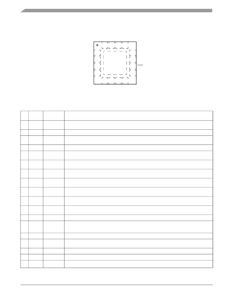
Pin Connections
16 15 14 13
V CC 1
V SS 2
I DATA 3
V SS 4
17
12 V SSA
11 V REGA
10 CS
9 V REG
5
6
7
8
Figure 4. Top View, 16-Pin QFN Package
Table 1. Pin Description
Pin
1
2
3
4
5
6
7
8
9
10
11
12
13
14
15
16
17
Pin
Name
V CC
V SS
I DATA
V SS
PCM
SCLK
D OUT
D IN
V REG
CS
V REGA
VSSA
V BUF
TEST
BUS_SW
VSSA
PAD
Corner
Pads
Formal Name
Supply
Digital GND
Response
Current
Digital GND
PCM
Output
SPI Clock
SPI Data Out
SPI Data In
Digital
Supply
Chip Select
Analog
Supply
Analog GND
Power
Supply
Test Pin
Bus Switch
Gate Drive
Analog GND
Die Attach Pad
Corner Pads
Definition
This pin is connected to the PSI5 power and data line through a resistor and supplies power to the device. An external capac-
itor must be connected between this pin and V SS . Reference Figure 1 .
This pin is the power supply return node for the digital circuitry.
This pin is connected to the PSI5 power and data line through a resistor and modulates the response current for PSI5 com-
munication. Reference Figure 1 .
This pin is the power supply return node for the digital circuitry.
This pin provides a 4 MHz PCM signal proportional to the acceleration data for test purposes. The output can be enabled via
OTP. Reference Section 3.5.3.7 . If unused, this pin must be left unconnected.
This input pin provides the serial clock to the SPI port for test purposes. An internal pulldown device is connected to this pin.
This pin must be grounded or left unconnected in the application.
This pin functions as the serial data output from the SPI port for test purposes. This pin must be left unconnected in the appli-
cation.
This pin functions as the serial data input to the SPI port for test purposes. An internal pulldown device is connected to this
pin. This pin must be grounded or left unconnected in the application.
This pin is connected to the power supply for the internal digital circuitry. An external capacitor must be connected between
this pin and V SS . Reference Figure 1 .
This input pin provides the chip select to the SPI port for test purposes. An internal pullup device is connected to this pin.This
pin must be left unconnected in the application.
This pin is connected to the power supply for the internal analog circuitry. An external capacitor must be connected between
this pin and V SSA . Reference Figure 1 .
This pin is the power supply return node for the analog circuitry.
This pin is connected to a buffer regulator for the internal circuitry. The buffer regulator supplies both the analog (V REGA ) and
digital (V REG ) supplies to provide immunity from EMC and supply dropouts on V CC . An external capacitor must be connected
between this pin and V SS . Reference Figure 1 .
This pin is must be grounded or left unconnected in the application.
This pin is the drive for a low-side daisy chain switch. When daisy chain mode is enabled, this pin is connected to the gate of
an n-channel FET which connects V SS to V SS_OUT. Reference Figure 1 . If unused, this pin must be left unconnected.
This pin is the power supply return node for the analog circuitry.
This pin is the die attach flag, and is internally connected to VSS. Reference Section 7 for die attach pad connection details.
The corner pads are internally connected to V SS .
MMA52xxKW
Sensors
4
Freescale Semiconductor, Inc.
发布紧急采购,3分钟左右您将得到回复。
相关PDF资料
MMA6331LT
SENSORS ACCELEROMETER 14LGA
MMA6341LT
IC ACCELER 3G/8G XY-AXIS 14LGA
MMA6361LT
IC ACCELER 1.5G XY-AXIS 14LGA
MMA6527KW
IC ACCELEROMETER XY AXIS 16QFN
MMA6556KW
IC ACCELEROMETER X AXIS 16QFN
MMA6826AKW
IC ACCELEROMETER XY AXIS 16QFN
MMA6854KW
IC ACCELEROMETER X AXIS 16QFN
MMA7331LR2
ACCELEROMETER 4G XYZ ENH 14-LGA
相关代理商/技术参数
MMA52XXAKW
制造商:FREESCALE 制造商全称:Freescale Semiconductor, Inc 功能描述:Xtrinsic MMA52xxAKW PSI5 Inertial Sensor
MMA52XXKW
制造商:FREESCALE 制造商全称:Freescale Semiconductor, Inc 功能描述:PSI5 Inertial Sensor
MMA52XXWR2
制造商:FREESCALE 制造商全称:Freescale Semiconductor, Inc 功能描述:PSI5 Inertial Sensor
MMA621010AEG
功能描述:加速计 - 板上安装 100/100G XY ANALOG RoHS:否 制造商:Murata 传感轴:Double 加速:12 g 灵敏度: 封装 / 箱体: 输出类型:Analog 数字输出 - 位数:11 bit 电源电压-最大:5.25 V 电源电压-最小:4.75 V 电源电流:4 mA 最大工作温度:+ 125 C 最小工作温度:- 40 C
MMA621010AEGR2
功能描述:加速计 - 板上安装 100/100G XY ANALOG RoHS:否 制造商:Murata 传感轴:Double 加速:12 g 灵敏度: 封装 / 箱体: 输出类型:Analog 数字输出 - 位数:11 bit 电源电压-最大:5.25 V 电源电压-最小:4.75 V 电源电流:4 mA 最大工作温度:+ 125 C 最小工作温度:- 40 C
MMA621010AKEG
功能描述:加速计 - 板上安装 100/100G XY ANALOG RoHS:否 制造商:Murata 传感轴:Double 加速:12 g 灵敏度: 封装 / 箱体: 输出类型:Analog 数字输出 - 位数:11 bit 电源电压-最大:5.25 V 电源电压-最小:4.75 V 电源电流:4 mA 最大工作温度:+ 125 C 最小工作温度:- 40 C
MMA621010AKEGR2
功能描述:加速计 - 板上安装 100/100G XY ANALOG RoHS:否 制造商:Murata 传感轴:Double 加速:12 g 灵敏度: 封装 / 箱体: 输出类型:Analog 数字输出 - 位数:11 bit 电源电压-最大:5.25 V 电源电压-最小:4.75 V 电源电流:4 mA 最大工作温度:+ 125 C 最小工作温度:- 40 C
MMA621010EG
功能描述:加速计 - 板上安装 100 /100 XY DIGITAL RoHS:否 制造商:Murata 传感轴:Double 加速:12 g 灵敏度: 封装 / 箱体: 输出类型:Analog 数字输出 - 位数:11 bit 电源电压-最大:5.25 V 电源电压-最小:4.75 V 电源电流:4 mA 最大工作温度:+ 125 C 最小工作温度:- 40 C
